Topic2:FPGA Design with Verilog FPGA Design Method Design flow tools Deign Model of Verilog HDL Design style of Verilog HDL Design Examples 。RTL level design Components of Datapath Components of Controller Supplementary 。Synthesizable 。Some experiences 。Other syntax rules 2021/1/13 ASIC Design,by Yan Bo 3
ASIC Design, by Yan Bo Topic2: FPGA Design with Verilog FPGA Design Method Design flow & tools Deign Model of Verilog HDL Design style of Verilog HDL Design Examples • RTL level design • Components of Datapath • Components of Controller Supplementary • Synthesizable • Some experiences • Other syntax rules 2021/1/13 3
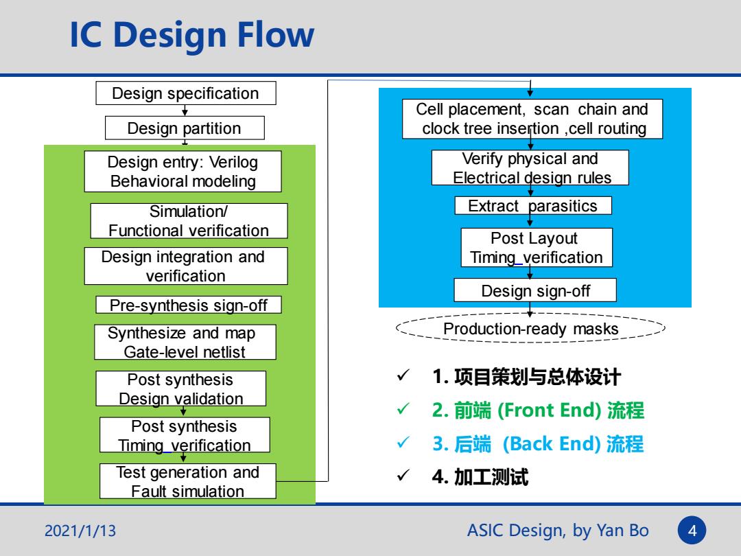
IC Design Flow Design specification Cell placement,scan chain and Design partition clock tree insertion cell routing Design entry:Verilog Verify physical and Behavioral modeling Electrical design rules Simulation/ Extract parasitics Functional verification Post Layout Design integration and Timing_verification verification Design sign-off Pre-synthesis sign-off Synthesize and map Production-ready masks Gate-level netlist Post synthesis 1.项目策划与总体设计 Design validation 2.前端(Front End)流程 Post synthesis Timing verification 3.后端(Back End)流程 Test generation and 4.加工测试 Fault simulation 2021/1/13 ASIC Design,by Yan Bo
ASIC Design, by Yan Bo Cell placement, scan chain and clock tree insertion ,cell routing Verify physical and Electrical design rules Extract parasitics Design sign-off Production-ready masks IC Design Flow Design partition Design entry: Verilog Behavioral modeling Simulation/ Functional verification Design integration and verification Pre-synthesis sign-off Synthesize and map Gate-level netlist Post synthesis Design validation Post synthesis Timing verification Test generation and Fault simulation Design specification Post Layout Timing verification ✓ 1. 项目策划与总体设计 ✓ 2. 前端 (Front End) 流程 ✓ 3. 后端 (Back End) 流程 ✓ 4. 加工测试 2021/1/13 4
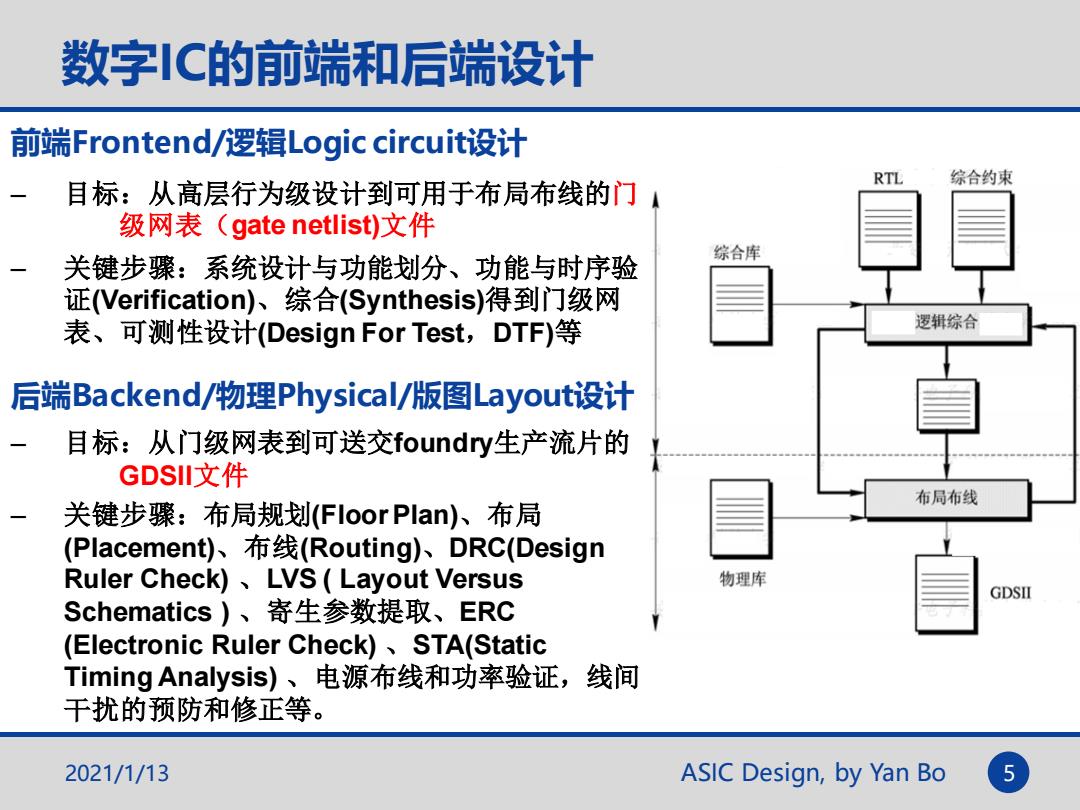
数字IC的前端和后端设计 前端Frontend/逻辑Logic circuit设计 RTL 综合约束 目标:从高层行为级设计到可用于布局布线的门 级网表(gate netlist)文件 综合库 关键步骤:系统设计与功能划分、功能与时序验 证(Verification)、综合(Synthesis)得到门级网 表、可测性设计(Design For Test,DTF)等 逻辑综合 后端Backend/物理Physical/版图Layout设计 目标:从门级网表到可送交foundry生产流片的 GDSl文件 布局布线 关键步骤:布局规划(Floor Plan)、布局 (Placement)、布线(Routing、DRC(Design Ruler Check)LVS(Layout Versus 物理库 GDSII Schematics)、寄生参数提取、ERC (Electronic Ruler Check)STA(Static Timing Analysis)、电源布线和功率验证,线间 干扰的预防和修正等。 2021/1/13 ASIC Design,by Yan Bo 5
ASIC Design, by Yan Bo 数字IC的前端和后端设计 前端Frontend/逻辑Logic circuit设计 – 目标:从高层行为级设计到可用于布局布线的门 级网表(gate netlist)文件 – 关键步骤:系统设计与功能划分、功能与时序验 证(Verification)、综合(Synthesis)得到门级网 表、可测性设计(Design For Test,DTF)等 后端Backend/物理Physical/版图Layout设计 – 目标:从门级网表到可送交foundry生产流片的 GDSII文件 – 关键步骤:布局规划(Floor Plan)、布局 (Placement)、布线(Routing)、DRC(Design Ruler Check) 、LVS ( Layout Versus Schematics ) 、寄生参数提取、ERC (Electronic Ruler Check) 、STA(Static Timing Analysis) 、电源布线和功率验证,线间 干扰的预防和修正等。 2021/1/13 5
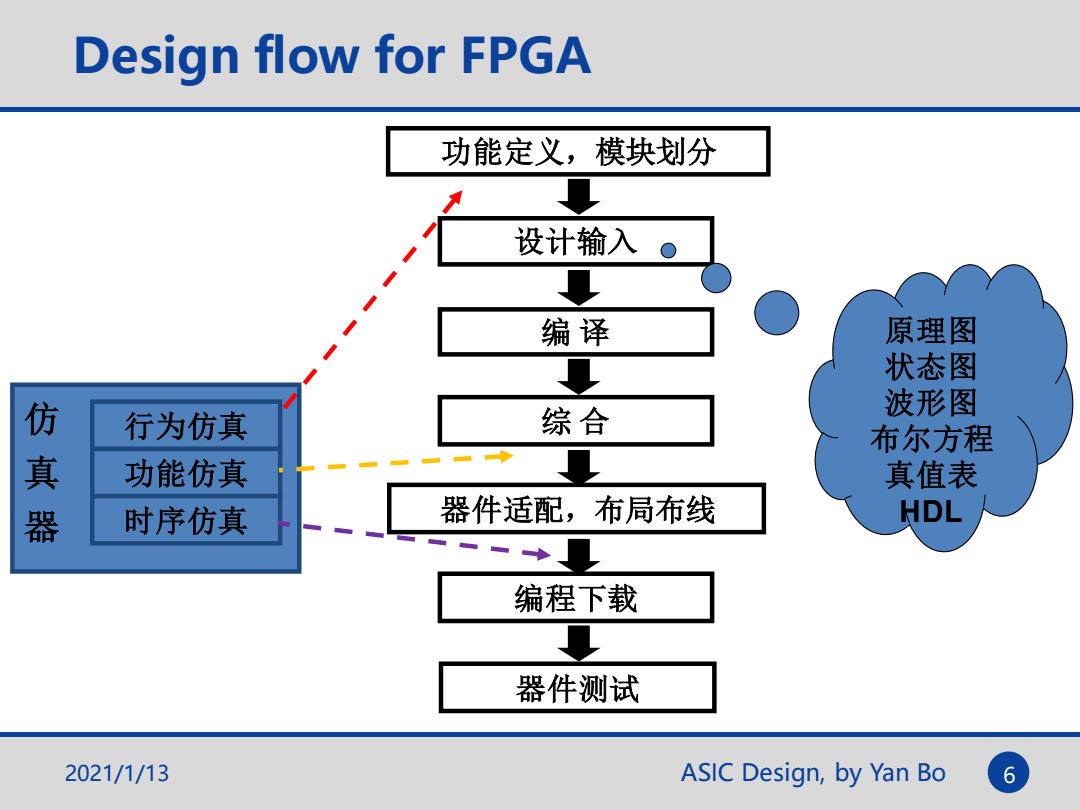
Design flow for FPGA 功能定义,模块划分 设计输入。 编译 原理图 状态图 波形图 行为仿真 综合 真 布尔方程 功能仿真 真值表 时序仿真 器件适配,布局布线 HDL 编程下载 器件测试 2021/1/13 ASIC Design,by Yan Bo 6
ASIC Design, by Yan Bo Design flow for FPGA 设计输入 综 合 编程下载 器件测试 仿 真 器 行为仿真 功能仿真 时序仿真 功能定义,模块划分 编 译 器件适配,布局布线 原理图 状态图 波形图 布尔方程 真值表 HDL 2021/1/13 6

Design flow for Full custom IC 功能定义,模块划分 设计输入 原理图 编译 状态图 波形图 综合 布尔方程 真值表 预布局 HDL 仿真 行为仿真 布局布线 功能仿真 版图生成、版图验证 时序仿真 可测性分析、测试生成 生产加工 硬件仿真 2021/1/13 ASIC Design,by Yan Bo 7
ASIC Design, by Yan Bo Design flow for Full custom IC 综 合 生产加工 硬件仿真 仿 真 器 行为仿真 功能仿真 时序仿真 功能定义,模块划分 编 译 布局布线 原理图 状态图 波形图 布尔方程 真值表 HDL 可测性分析、测试生成 预布局 设计输入 版图生成、版图验证 2021/1/13 7