Topic2:FPGA Design with Verilog FPGA Design Method Design flow tools Deign Model of Verilog HDL Design style of Verilog HDL Design Examples 。RTL level design Components of Datapath Components of Controller Supplementary ·Synthesizable 。Some experiences 。Other syntax rules 2021/1/13 ASIC Design,by Yan Bo 3
ASIC Design, by Yan Bo Topic2: FPGA Design with Verilog FPGA Design Method Design flow & tools Deign Model of Verilog HDL Design style of Verilog HDL Design Examples • RTL level design • Components of Datapath • Components of Controller Supplementary • Synthesizable • Some experiences • Other syntax rules 2021/1/13 3
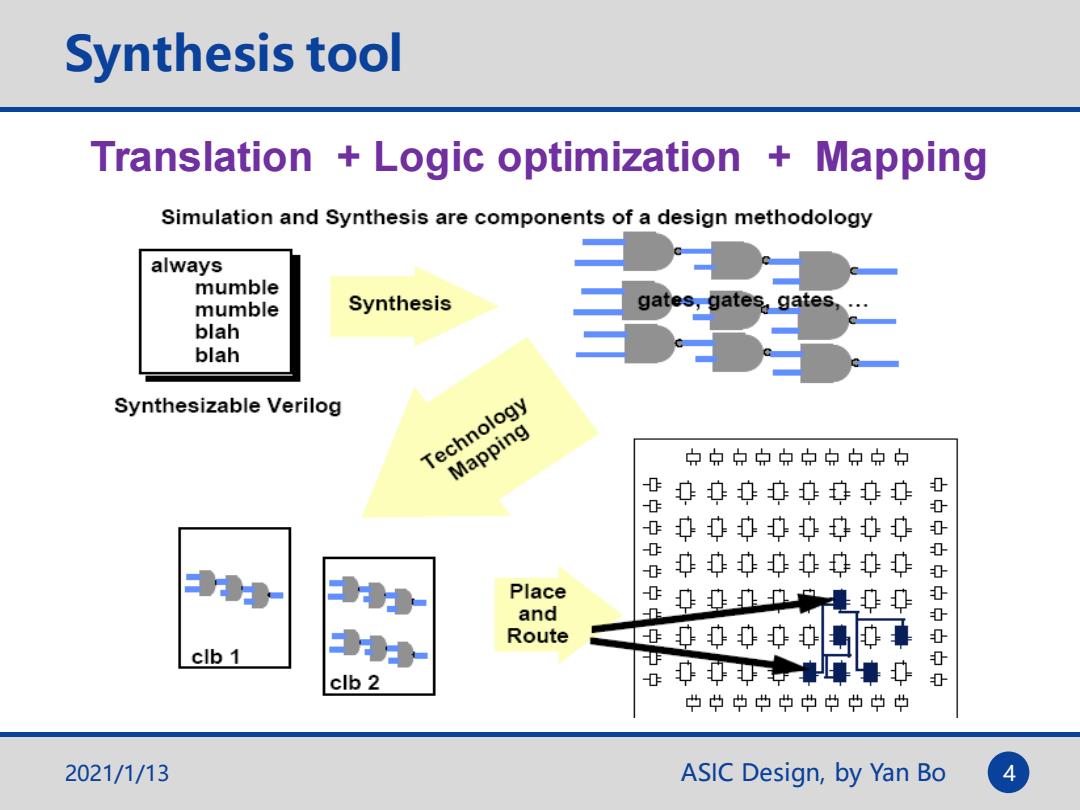
Synthesis tool Translation Logic optimization Mapping Simulation and Synthesis are components of a design methodology always mumble mumble Synthesis gates,gates,gates, blah blah Synthesizable Verilog Technology Mapping 白白白白白白白白白白 800000000 0中中中中中中中中 0 中中中中中中中中 Place and 00n是09 0 Route clb1 clb2 中中中中中中中单中中 2021/1/13 ASIC Design,by Yan Bo
ASIC Design, by Yan Bo Synthesis tool 2021/1/13 4 Translation + Logic optimization + Mapping
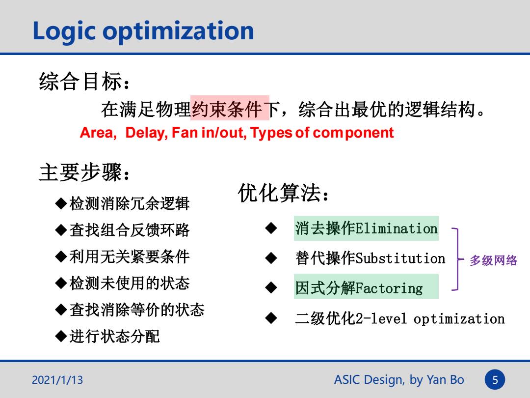
Logic optimization 综合目标: 在满足物理约束条件下,综合出最优的逻辑结构。 Area,Delay,Fan in/out,Types of component 主要步骤: 优化算法: ◆检测消除冗余逻辑 ◆查找组合反馈环路 消去操作Elimination ◆利用无关紧要条件 替代操作Substitution ,上多级网络 ◆检测未使用的状态 因式分解Factoring ◆查找消除等价的状态 二级优化2-level optimization ◆进行状态分配 2021/1/13 ASIC Design,by Yan Bo 5
ASIC Design, by Yan Bo Logic optimization 2021/1/13 5 主要步骤: ◆检测消除冗余逻辑 ◆查找组合反馈环路 ◆利用无关紧要条件 ◆检测未使用的状态 ◆查找消除等价的状态 ◆进行状态分配 综合目标: 在满足物理约束条件下,综合出最优的逻辑结构。 Area, Delay, Fan in/out, Types of component 优化算法: ◆ 消去操作Elimination ◆ 替代操作Substitution ◆ 因式分解Factoring ◆ 二级优化2-level optimization 多级网络
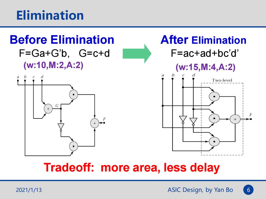
Elimination Before Elimination After Elimination F=Ga+G'b,G=c+d F=ac+ad+bc'd' w:10,M:2,A:2) (w:15,M:4,A:2) b c a Two-level Tradeoff:more area,less delay 2021/1/13 ASIC Design,by Yan Bo 6
ASIC Design, by Yan Bo Elimination 2021/1/13 6 After Elimination F=ac+ad+bc’d’ Before Elimination F=Ga+G’b, G=c+d (w:10,M:2,A:2) (w:15,M:4,A:2) Tradeoff: more area, less delay
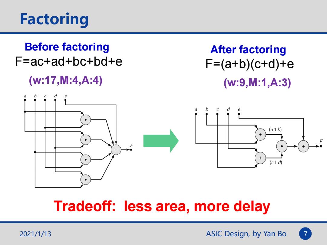
Factoring Before factoring After factoring F=ac+ad+bc+bd+e F=(a+b)(c+d)+e w:17,M:4,A:4) (W:9,M:1,A:3) b (a1b) (c1d) Tradeoff:less area,more delay 2021/1/13 ASIC Design,by Yan Bo 7
ASIC Design, by Yan Bo Factoring 2021/1/13 7 Tradeoff: less area, more delay After factoring F=(a+b)(c+d)+e Before factoring F=ac+ad+bc+bd+e (w:17,M:4,A:4) (w:9,M:1,A:3)