
第二讲 CMOS器件 游飞博导,副教授 电子科学与工程学院,feiyou@uestc.edu.cn 22西/
2020/3/7 1 第二讲 CMOS器件 游飞 博导,副教授 电子科学与工程学院, feiyou@uestc.edu.cn
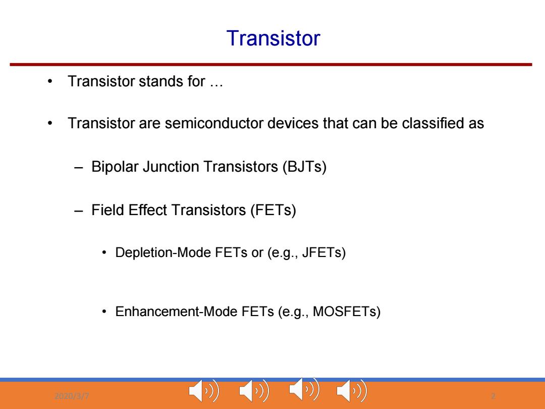
Transistor Transistor stands for .. Transistor are semiconductor devices that can be classified as -Bipolar Junction Transistors (BJTs) Field Effect Transistors(FETs) Depletion-Mode FETs or(e.g.,JFETs) Enhancement-Mode FETs(e.g.,MOSFETs) 西7
2020/3/7 2 SM 11 EECE 488 ± Set 1: Introduction and Background Transistor Transistor stands for « Transistor are semiconductor devices that can be classified as ± Bipolar Junction Transistors (BJTs) ± Field Effect Transistors (FETs) Depletion-Mode FETs or (e.g., JFETs) Enhancement-Mode FETs (e.g., MOSFETs)
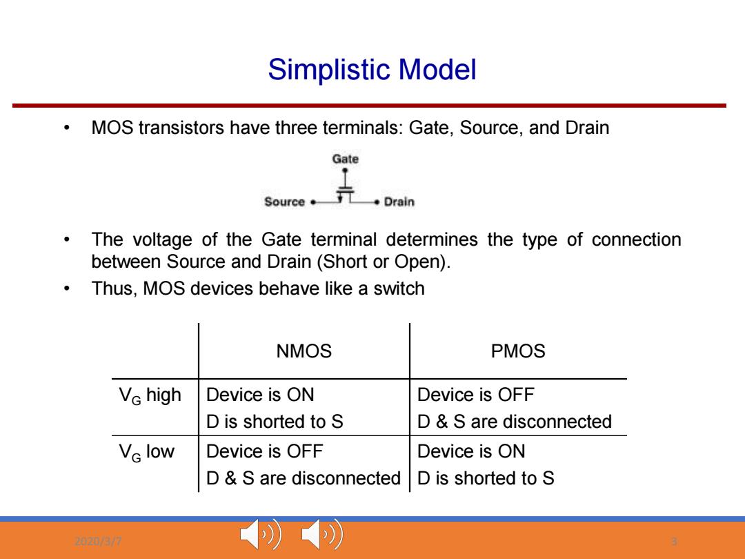
Simplistic Model MOS transistors have three terminals:Gate,Source,and Drain Gate Souw,六an The voltage of the Gate terminal determines the type of connection between Source and Drain (Short or Open). Thus,MOS devices behave like a switch NMOS PMOS Ve high Device is ON Device is OFF D is shorted to S D S are disconnected Ve low Device is OFF Device is ON D &S are disconnected D is shorted to S 2西3/7
2020/3/7 3 SM 12 EECE 488 ± Set 1: Introduction and Background Simplistic Model MOS transistors have three terminals: Gate, Source, and Drain The voltage of the Gate terminal determines the type of connection between Source and Drain (Short or Open). Thus, MOS devices behave like a switch Device is ON D is shorted to S Device is OFF D & S are disconnected VG low Device is OFF D & S are disconnected Device is ON D is shorted to S VG high NMOS PMOS
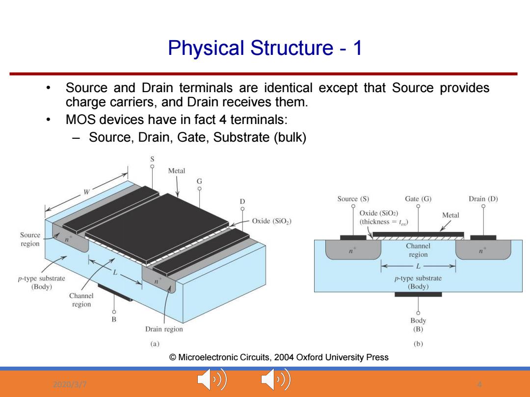
Physical Structure 1 。 Source and Drain terminals are identical except that Source provides charge carriers,and Drain receives them. MOS devices have in fact 4 terminals: Source,Drain,Gate,Substrate (bulk) Q Metal D Source (S) Gate (G) Drain (D) 0 0 Q Oxide (SiO2) Metal Oxide (SiO2) (thickness fax) Source region Channel n n region -L p-type substrate p-type substrate (Body) (Body) Channel region B Body Drain region (B) (a) (b) Microelectronic Circuits,2004 Oxford University Press 心2西/
2020/3/7 4 SM 13 EECE 488 ± Set 1: Introduction and Background Physical Structure - 1 Source and Drain terminals are identical except that Source provides charge carriers, and Drain receives them. MOS devices have in fact 4 terminals: ± Source, Drain, Gate, Substrate (bulk) © Microelectronic Circuits, 2004 Oxford University Press
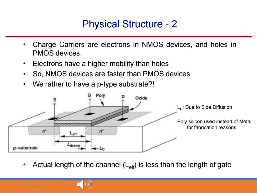
Physical Structure -2 Charge Carriers are electrons in NMOS devices,and holes in PMOS devices. 。 Electrons have a higher mobility than holes So,NMOS devices are faster than PMOS devices We rather to have a p-type substrate?! G Poly Oxide Lp:Due to Side Diffusion Poly-silicon used instead of Metal for fabrication reasons p-substrate drawn -Lo Actual length of the channel (Lef)is less than the length of gate 西/7
SM2020/3/7 5 14 EECE 488 ± Set 1: Introduction and Background Physical Structure - 2 LD: Due to Side Diffusion Poly-silicon used instead of Metal for fabrication reasons Actual length of the channel (Leff) is less than the length of gate Charge Carriers are electrons in NMOS devices, and holes in PMOS devices. Electrons have a higher mobility than holes So, NMOS devices are faster than PMOS devices We rather to have a p-type substrate?!