
VISHAY. IRFP450,SiHFP450 Vishay Siliconix Power MOSFET FEATURES PRODUCT SUMMARY ·Dynamic dV/dt Rating Vos (V) 500 Ves=10V Repetitive Avalanche Rated RDsion)() 0.40 Qg(Max.)(nC) 150 Isolated Central Mounting Hole RoHS* Qgs(nC) 20 ·Fast Switching COMPLIANT Qgd(nC) 80 ·Ease of Paralleling Configuration Single Simple Drive Requirements 0 Lead(Pb)-free Available ● T0-247 DESCRIPTION Third generation Power MOSFETs from Vishay provide the designer with the best combination of fast switching, ruggedized device design,low on-resistance and cost-effectiveness. The TO-247 package is preferred for commercial-industrial applications where higher power levels preclude the use of TO-220 devices.The TO-247 is similar but superior to the N-Channel MOSFET earlier TO-218 package because its isolated mounting hole It also provides greater creepage distances between pins to meet the requirements of most safety specifications. ORDERING INFORMATION Package T0-247 IRFP450PbF Lead(Pb)-free SiHFP450-E3 SnPb IRFP450 SiHFP450 ABSOLUTE MAXIMUM RATINGS Tc =25C,unless otherwise noted PARAMETER SYMBOL LIMIT UNIT Drain-Source Voltage Vos 500 Gate-Source Voltage Vas ±20 Continuous Drain Current VGs at 10V Tc=25℃ 14 Tc=100C p 8.7 Pulsed Drain Currenta IDM 56 Linear Derating Factor 1.5 W/C Single Pulse Avalanche Energyb EAS 760 mJ Repetitive Avalanche Currenta IAR 8.7 A Repetitive Avalanche Energya EAR 19 mJ Maximum Power Dissipation Tc=25℃ Po 190 W Peak Diode Recovery dV/dte dV/dt 3.5 V/ns Operating Junction and Storage Temperature Range TJ,Tstg -55to+150 300d ℃ Soldering Recommendations(Peak Temperature) for 10s 10 Ibf.in Mounting Torque 6-32 or M3 screw 1.1 N.m Notes a.Repetitive rating;pulse width limited by maximum junction temperature (see fig.11). b.Vpp=50 V,starting TJ=25C,L=7.0 mH,RG =25 2,IAS=14 A (see fig.12). c.lso≤14A,dWt≤130AWμs,Vop≤Vos,Ty≤150C. d.1.6 mm from case. Pb containing terminations are not RoHS compliant,exemptions may apply Document Number:91233 www.vishay.com S-81271-Rev.A.16-Jun-08 1
Document Number: 91233 www.vishay.com S-81271-Rev. A, 16-Jun-08 1 Power MOSFET IRFP450, SiHFP450 Vishay Siliconix FEATURES • Dynamic dV/dt Rating • Repetitive Avalanche Rated • Isolated Central Mounting Hole • Fast Switching • Ease of Paralleling • Simple Drive Requirements • Lead (Pb)-free Available DESCRIPTION Third generation Power MOSFETs from Vishay provide the designer with the best combination of fast switching, ruggedized device design, low on-resistance and cost-effectiveness. The TO-247 package is preferred for commercial-industrial applications where higher power levels preclude the use of TO-220 devices. The TO-247 is similar but superior to the earlier TO-218 package because its isolated mounting hole. It also provides greater creepage distances between pins to meet the requirements of most safety specifications. Notes a. Repetitive rating; pulse width limited by maximum junction temperature (see fig. 11). b. VDD = 50 V, starting TJ = 25 °C, L = 7.0 mH, RG = 25 Ω, IAS = 14 A (see fig. 12). c. ISD ≤ 14 A, dI/dt ≤ 130 A/µs, VDD ≤ VDS, TJ ≤ 150 °C. d. 1.6 mm from case. PRODUCT SUMMARY VDS (V) 500 RDS(on) (Ω) VGS = 10 V 0.40 Qg (Max.) (nC) 150 Qgs (nC) 20 Qgd (nC) 80 Configuration Single N-Channel MOSFET G D S TO-247 G D S Available RoHS* COMPLIANT ORDERING INFORMATION Package TO-247 Lead (Pb)-free IRFP450PbF SiHFP450-E3 SnPb IRFP450 SiHFP450 ABSOLUTE MAXIMUM RATINGS TC = 25 °C, unless otherwise noted PARAMETER SYMBOL LIMIT UNIT Drain-Source Voltage VDS 500 V Gate-Source Voltage VGS ± 20 Continuous Drain Current VGS at 10 V TC = 25 °C ID 14 TC = 100 °C 8.7 A Pulsed Drain Currenta IDM 56 Linear Derating Factor 1.5 W/°C Single Pulse Avalanche Energyb EAS 760 mJ Repetitive Avalanche Currenta IAR 8.7 A Repetitive Avalanche Energya EAR 19 mJ Maximum Power Dissipation TC = 25 °C PD 190 W Peak Diode Recovery dV/dtc dV/dt 3.5 V/ns Operating Junction and Storage Temperature Range TJ, Tstg - 55 to + 150 °C Soldering Recommendations (Peak Temperature) for 10 s 300d Mounting Torque 6-32 or M3 screw 10 lbf · in 1.1 N · m * Pb containing terminations are not RoHS compliant, exemptions may apply
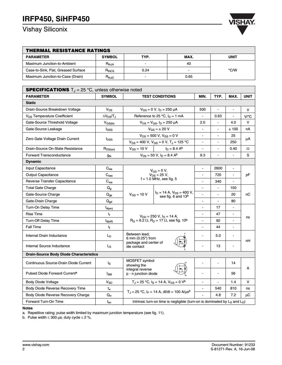
IRFP450,SiHFP450 VISHAY Vishay Siliconix THERMAL RESISTANCE RATINGS PARAMETER SYMBOL TYP. MAX. UNIT Maximum Junction-to-Ambient RthJA 40 Case-to-Sink,Flat,Greased Surface Rthcs 0.24 C/W Maximum Junction-to-Case (Drain) RthJc 0.65 SPECIFICATIONS TJ=25C,unless otherwise noted PARAMETER SYMBOL TEST CONDITIONS MIN. TYP.MAX.UNIT Static Drain-Source Breakdown Voltage Vos VGs=0V,lD=250μA 500 - V Vps Temperature Coefficient △Vps/Tj Reference to 25C,lp=1 mA 0.63 、 VC Gate-Source Threshold Voltage VGs(th) VDs VGS,Ip=250 HA 2.0 4.0 V Gate-Source Leakage lGss VGs=±20V ±100 nA Vos =500 V,Vas =0V 25 Zero Gate Voltage Drain Current Ioss μA VDs=400 V,Ves=0 V,TJ=125C 、 250 Drain-Source On-State Resistance Rps(on) VGs =10 V Ip =8.4 Ab 0.40 Forward Transconductance 9ts VDs=50 V,lo=8.4 A5 9.3 Dynamic Input Capacitance Ciss Ves=0V, 2600 Output Capacitance Coss Vos =25 V, 720 pF Reverse Transfer Capacitance Crss f=1.0 MHz,see fig.5 340 Total Gate Charge Qg 150 Gate-Source Charge Qgs VGs=10V ID =14 A,VDs =400 V, see fig.6 and 13b 20 nC Gate-Drain Charge Qgd 80 Turn-On Delay Time tdlon) 17 、 Rise Time t VDD =250 V,Ip=14 A, 47 ns Turn-Off Delay Time td(off) RG 6.2 Q,Ro=17Q,see fig.10b 92 Fall Time 44 Internal Drain Inductance Lo Between lead, 5.0 6 mm (0.25")from package and center of nH nternal Source Inductance Ls die contact 13 Drain-Source Body Diode Characteristics Continuous Source-Drain Diode Current g MOSFET symbol 14 showing the integral reverse Pulsed Diode Forward Currenta IsM p-n junction diode 56 Body Diode Voltage Vsp TJ=25℃,ls=14A,VGs=0V 1.4 V Body Diode Reverse Recovery Time tm 540 810 ns TJ-25℃,lF-14Ad/dt=100A/μsb Body Diode Reverse Recovery Charge Qrt 4.8 7.2μC Forward Turn-On Time ton Intrinsic turn-on time is negligible(turn-on is dominated by Ls and Lp) Notes a.Repetitive rating;pulse width limited by maximum junction temperature(see fig.11). b.Pulse width≤300us;duty cycle≤2%. www.vishay.com Document Number:91233 S-81271-Rev.A,16-Jun-08
www.vishay.com Document Number: 91233 2 S-81271-Rev. A, 16-Jun-08 IRFP450, SiHFP450 Vishay Siliconix Notes a. Repetitive rating; pulse width limited by maximum junction temperature (see fig. 11). b. Pulse width ≤ 300 µs; duty cycle ≤ 2 %. THERMAL RESISTANCE RATINGS PARAMETER SYMBOL TYP. MAX. UNIT Maximum Junction-to-Ambient RthJA - 40 Case-to-Sink, Flat, Greased Surface RthCS 0.24 - °C/W Maximum Junction-to-Case (Drain) RthJC - 0.65 SPECIFICATIONS TJ = 25 °C, unless otherwise noted PARAMETER SYMBOL TEST CONDITIONS MIN. TYP. MAX. UNIT Static Drain-Source Breakdown Voltage VDS VGS = 0 V, ID = 250 µA 500 - - V VDS Temperature Coefficient ΔVDS/TJ Reference to 25 °C, ID = 1 mA - 0.63 - V/°C Gate-Source Threshold Voltage VGS(th) VDS = VGS, ID = 250 µA 2.0 - 4.0 V Gate-Source Leakage IGSS VGS = ± 20 V - - ± 100 nA Zero Gate Voltage Drain Current IDSS VDS = 500 V, VGS = 0 V - - 25 µA VDS = 400 V, VGS = 0 V, TJ = 125 °C - - 250 Drain-Source On-State Resistance RDS(on) VGS = 10 V ID = 8.4 Ab - - 0.40 Ω Forward Transconductance gfs VDS = 50 V, ID = 8.4 Ab 9.3 - - S Dynamic Input Capacitance Ciss VGS = 0 V, VDS = 25 V, f = 1.0 MHz, see fig. 5 - 2600 - Output Capacitance Coss - 720 - pF Reverse Transfer Capacitance Crss - 340 - Total Gate Charge Qg VGS = 10 V ID = 14 A, VDS = 400 V, see fig. 6 and 13b - - 150 Gate-Source Charge Qgs - - 20 nC Gate-Drain Charge Qgd - - 80 Turn-On Delay Time td(on) VDD = 250 V, ID = 14 A, RG = 6.2 Ω, RD = 17 Ω, see fig. 10b - 17 - ns Rise Time tr - 47 - Turn-Off Delay Time td(off) - 92 - Fall Time tf - 44 - Internal Drain Inductance LD Between lead, 6 mm (0.25") from package and center of die contact - 5.0 - nH Internal Source Inductance LS - 13 - Drain-Source Body Diode Characteristics Continuous Source-Drain Diode Current IS MOSFET symbol showing the integral reverse p - n junction diode - - 14 A Pulsed Diode Forward Currenta ISM - - 56 Body Diode Voltage VSD TJ = 25 °C, IS = 14 A, VGS = 0 Vb - - 1.4 V Body Diode Reverse Recovery Time trr TJ = 25 °C, IF = 14 A, dI/dt = 100 A/µsb - 540 810 ns Body Diode Reverse Recovery Charge Qrr - 4.8 7.2 µC Forward Turn-On Time ton Intrinsic turn-on time is negligible (turn-on is dominated by LS and LD) D S G S D G

VISHAY. IRFP450,SiHFP450 Vishay Siliconix TYPICAL CHARACTERISTICS 25C,unless otherwise noted 1500 0 6 4.5- 20us PULSE WIDTH 「c=250c -20us PULSE WIDTH 10 09 101 8 0 Vps,Drain-to-Source Voltage (volts) VGs,Gate-to-Source Voltage (volts) Fig.1-Typical Output Characteristics,Tc =25C Fig.3-Typical Transfer Characteristics 3.5 0=14a 3.0 2.5 2.0 1,5 1.0 0.5 20Us PULSE WIDTH Tc■1500C 0 VGS 10V 100 101 0.0 60-40-20020406060100120140160 Vps,Drain-to-Source Voltage (volts) TJ,Junction Temperature(C) Fig.2-Typical Output Characteristics,Tc=150C Fig.4-Normalized On-Resistance vs.Temperature Document Number:91233 www.vishay.com S-81271-Rev.A.16-Jun-08 3
Document Number: 91233 www.vishay.com S-81271-Rev. A, 16-Jun-08 3 IRFP450, SiHFP450 Vishay Siliconix TYPICAL CHARACTERISTICS 25 °C, unless otherwise noted Fig. 1 - Typical Output Characteristics, TC = 25 °C Fig. 2 - Typical Output Characteristics, TC = 150 °C Fig. 3 - Typical Transfer Characteristics Fig. 4 - Normalized On-Resistance vs. Temperature

IRFP450,SiHFP450 VISHAY Vishay Siliconix VGS OV,T 1MHZ 0155= Cas SHOATED 5000 Crss O 400 C15 300 200 Co5 250g P55 1000 岛 VGS OV 12 1. 2.0 Vps,Drain-to-Source Voltage (volts) Vsp,Source-to-Drain Voltage (volts) Fig.5-Typical Capacitance vs.Drain-to-Source Voltage Fig.7-Typical Source-Drain Diode Forward Voltage 8 103 1D.14a Cs400 CPERATION IN THIS AREA LIMITED c52507 BY ROs (ON) 5:100 10 10 c=25°6 FOR TEST CIRCUIT T.=1500C SEE FIGURE 13 SINGLE PULSE 20 40 90100120 140 0.1 2 510 2 5 10225. 10 QG,Total Gate Charge (nC) Vps,Drain-to-Source Voltage (volts) Fig.6-Typical Gate Charge vs.Gate-to-Source Voltage Fig.8-Maximum Safe Operating Area www.vishay.com Document Number:91233 S-81271-Rev.A,16-Jun-08
www.vishay.com Document Number: 91233 4 S-81271-Rev. A, 16-Jun-08 IRFP450, SiHFP450 Vishay Siliconix Fig. 5 - Typical Capacitance vs. Drain-to-Source Voltage Fig. 6 - Typical Gate Charge vs. Gate-to-Source Voltage Fig. 7 - Typical Source-Drain Diode Forward Voltage Fig. 8 - Maximum Safe Operating Area

VISHAY. IRFP450,SiHFP450 Vishay Siliconix Rp Vos> D.U.T. R 几1ov Pulse widths 1 us Duty factor s0.1% Fig.10a-Switching Time Test Circuit 6 Vos 90% 25 50 75 400 125 150 10% Tc,Case Temperature(C) td(alf)4 Fig.9-Maximum Drain Current vs.Case Temperature Fig.10b-Switching Time Waveforms 0.1 SINGLE PULSE NOTES: -1.DUTY FACTOR,D-t1/t2 2.PEAK T;-PDM x Zthjc Tc o 105 10 10▣ 102 0.1 10 t1,Rectangular Pulse Duration (seconds) Fig.11-Maximum Effective Transient Thermal Impedance,Junction-to-Case Vary to obtain Vos required IAs Ra D.U.T 4 AS 10V 0.012 Fig.12a-Unclamped Inductive Test Circuit Fig.12b-Unclamped Inductive Waveforms Document Number:91233 www.vishay.com S-81271-Rev.A.16-Jun-08 5
Document Number: 91233 www.vishay.com S-81271-Rev. A, 16-Jun-08 5 IRFP450, SiHFP450 Vishay Siliconix Fig. 9 - Maximum Drain Current vs. Case Temperature Fig. 10a - Switching Time Test Circuit Fig. 10b - Switching Time Waveforms Fig. 11 - Maximum Effective Transient Thermal Impedance, Junction-to-Case Fig. 12a - Unclamped Inductive Test Circuit Fig. 12b - Unclamped Inductive Waveforms Pulse width ≤ 1 µs Duty factor ≤ 0.1 % RD VGS RG D.U.T. 10 V + - VDS VDD VDS 90 % 10 % VGS t d(on) t r t d(off) t f RG IAS tp 0.01 Ω D.U.T L VDS + - VDD A 10 V Vary tp to obtain required IAS IAS VDS VDD VDS tp