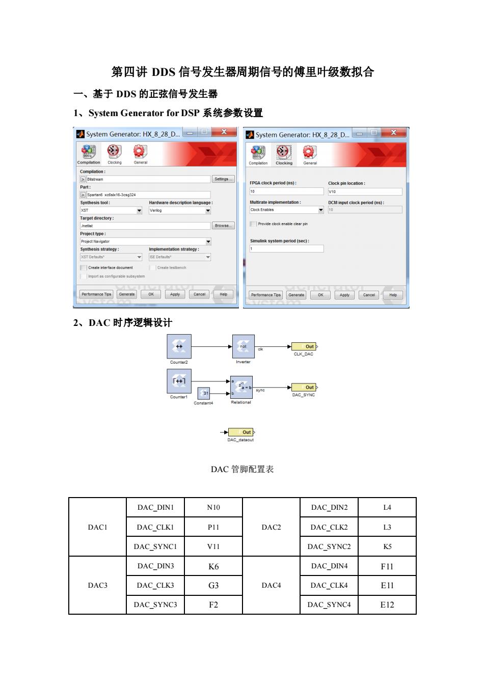
第四讲DDS信号发生器周期信号的傅里叶级数拟合 一、基于DDS的正弦信号发生器 1、System Generator for DSP系统参数设置 ☑System Generator.HX828.D.-▣x System Generator:HX 8 28 D. 盟 Compilation Clockng General Compilation Clocking General Compilation: Part: FPGA clock period (ns): Clock pin location: Spartan6 xc5sb16-3csg324 10 V10 Synthesis tool: Hardware description language DCM input clock period (ns): XST Clock Enabies 10 Target directory: metist B/0w88 Provide clack enable clear pin Project type: Proct Navigtor Simulink system period(sec): Synthesis strategy: Implementation strategy: Defauts' SE Dera.ts' Creste nterface document Create testenh mport as configurable subsystem Pertormance Tps Generate OK Apply Cancel Helo Performance Tos Generate OK Appty Cancet Hetb 2、DAC时序逻辑设计 Out CLK_DAC +1 Out Counter' DAC_SYNC Out DAC_dataout DAC管脚配置表 DAC DINI N10 DAC DIN2 L4 DACI DAC CLKI P11 DAC2 DAC CLK2 L3 DAC SYNCI VIl DAC SYNC2 K5 DAC DIN3 K6 DAC DIN4 F11 DAC3 DAC_CLK3 G3 DAC4 DAC_CLK4 E11 DAC_SYNC3 F2 DAC_SYNC4 E12
第四讲 DDS 信号发生器周期信号的傅里叶级数拟合 一、基于 DDS 的正弦信号发生器 1、System Generator for DSP 系统参数设置 2、DAC 时序逻辑设计 DAC 管脚配置表 DAC1 DAC_DIN1 N10 DAC2 DAC_DIN2 L4 DAC_CLK1 P11 DAC_CLK2 L3 DAC_SYNC1 V11 DAC_SYNC2 K5 DAC3 DAC_DIN3 K6 DAC4 DAC_DIN4 F11 DAC_CLK3 G3 DAC_CLK4 E11 DAC_SYNC3 F2 DAC_SYNC4 E12
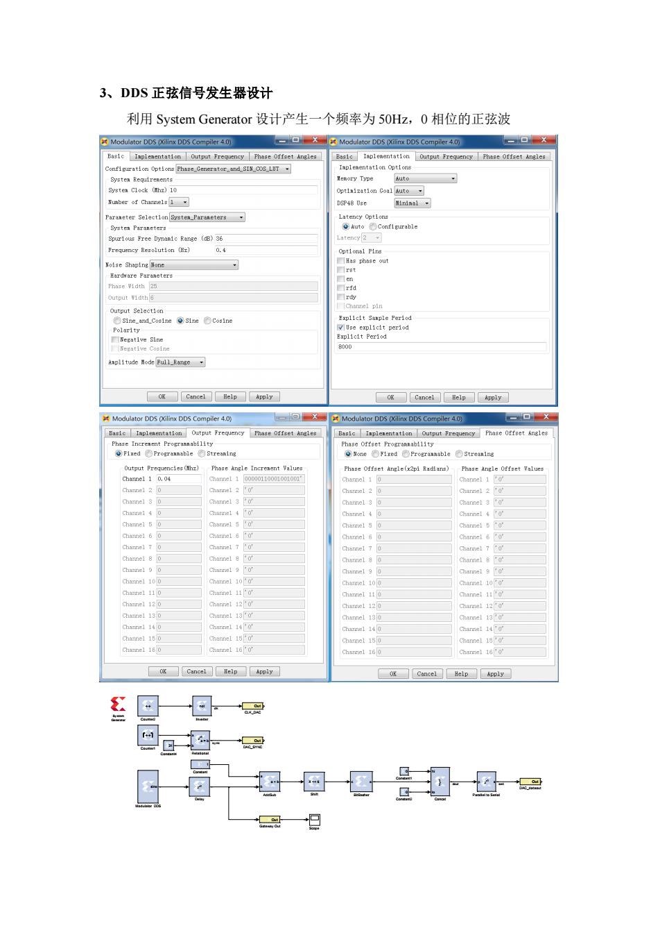
3、DDS正弦信号发生器设计 利用System Generator设计产生一个频率为50Hz,0相位的正弦波 Modulator DDSinx DDS Compier.) Modulator DDS (Xilinx DDS Compiler 4.0) -▣X Basic Iapleaentation Output Frequency Fhase Offset Angles Basic Inplenentation Output Frequency Fhase Offset Angles Configuration Options Fhase_Generator_and_SIN_COS_LUT Iapleaentation Options Systea Recuirenents enory Type Auto Systea Clock (Mhz)10 Optiaization Goal Auto Sumber of Charnels1 DSP48 Use Nininal Paraneter Selection Systea_Paraneters Latency Options Syatea Paraneters Auto Configurable Spurlous Free Dynanic Range (dB)36 Latency 2 Frequency Resolution (Hz) 0.4 Optional Pins Noise Shaping None Has phase out rBt Hardware Paraneters cm Phase Vidth 25 rfd Output餐1dthG ■rw output Selection Channel pin wsi2_and_Coeine⊙s1ne©Cosine Explicit Sanple Period Polarity Use explicit period Begative Sine Explicit Period Begative Coaine 000 Amplitude Mode Full_Range o Cancel Help Apply og☐CancelBe1 Apply Modulator DDS (Xilinx DDS Compiler 4.0) L-回Xas Modulator DDS xilinx DDS Compiler4.O 一▣X Basic Iaplenentation Output Frequency Phase offset Angles Basic Iaplesentation Output Frequency Phase Offset Angles Phase Increnent Progrannability Phase oftset frogranmability Fixed Progrannable Streaning Output Frequencies (Mhz) Phase Angle Increaent Yalues Fhase Offset Angle(x2pi Radians) Fhase Angle Offset Values Channel 1 0.04 am1100000110001001001 Charmel 1 0 Channel 2 0 Charetel 2 0 Channel 20' Channel 30 Charnel 3 0 Charmel to' Charnel4 0 Channel 50 Channel 60 Channel 60' Channel 70 Channel 7 0' Channel 80 Channel 9 0 Channel 9 Channel 100 Channel 100 Channel 11 0 Channel 110' Channel 110' Channel 120 Channel 120 Channel 120' Channel 13 0 Channel 130' Channel 140 Charnel 140 Channel 140' Channel 150 Channel 180' Charmel 150 Chanel 15o' Channel 16 0 Charmel 160 OK Cancel OK Cancel Help Bpply ≤回一回 回旦超层 国母县&母是
3、DDS 正弦信号发生器设计 利用 System Generator 设计产生一个频率为 50Hz,0 相位的正弦波 X << 6 Shift Scope a b a = b z - 1 Relational p z s - 1 Parallel to Serial sine Modulator DDS not Inverter Out Gateway Out z - 1 Delay Out DAC_dataout Out DAC_SYNC ++ Counter2 ++ Counter1 3 1 Constant4 0 Constant2 0 Constant1 1 Constant h i l o } Concat Out CLK_DAC c a BitBasher a b a + b AddSub Sy stem Generator sy nc clk dout seri

rig'd 12.00V 10.0ms 100kS/s 17 31Mar2014 T+y0.00000s 10k points 840mV 15:26:03 二、利用傅里叶级数拟合周期信号 例41:将下图所示方波信号展开为傅里叶级数。 f(t) 2 E 解:(1)数学计算 按题意方波信号在一个周期内的解析式为 E 2 -5s1<0 f0= E-2 0≤1≤乃 分别求得傅里叶系数: a.-(5}cosd+号(}comm/灿 -d7儿a+kaar]-0
二、利用傅里叶级数拟合周期信号 例 4-1:将下图所示方波信号展开为傅里叶级数。 解:(1)数学计算 按题意方波信号在一个周期内的解析式为 ( ) − − = 2 0 2 0 2 2 t T E T t E f t 分别求得傅里叶系数: cos 2 2 cos 2 2 2 0 0 0 2 0 + = − − T n T n tdt E T n tdt E T a ( sin ) (sin ) 0 n E 2 0 0 0 0 2 0 = − + = − T T n t n t T

a=子}sin,d+子((}sinn,d 5asnee+(sg E[2-2cos(nx】 「2E n为奇数 即: b= nπ 10 n为偶数 故得信号的傅里叶级数展开式为 f(0)= 2E π sino+3sin30/+亏sin5o1+.+sin n/+. 它只含有一、三、五、.等奇次谐波分量。 (2)Matlab仿真 4=2π6,令6=50h,T=1s,E=1. 50 100 150 200 250 300 0 0 50 100 150 200 250 300 50 100 150 200 250 300 50 100 150 200 250 300 clc,clear;
+ = − − 2 0 0 0 2 0 sin 2 2 sin 2 2 T n T n tdt E T n tdt E T b ( ) ( ) 2 0 0 0 0 2 0 cos cos n E T T n t n t T = + − − ( ) n n E 2 2cos 2 = − 即: = 为偶数 为奇数 n n n E bn 0 2 故得信号的傅里叶级数展开式为 ( ) 0 0 0 0 2 1 1 1 sin sin 3 sin5 sin 3 5 E f t t t t n t n = + + + + + 它只含有一、三、五、.等奇次谐波分量。 (2)Matlab 仿真 0 0 = 2 f ,令 0 f Hz = 50 ,T s = 1 , E =1。 0 50 100 150 200 250 300 - 1 0 1 0 50 100 150 200 250 300 - 1 0 1 0 50 100 150 200 250 300 - 1 0 1 0 50 100 150 200 250 300 - 1 0 1 clc,clear;
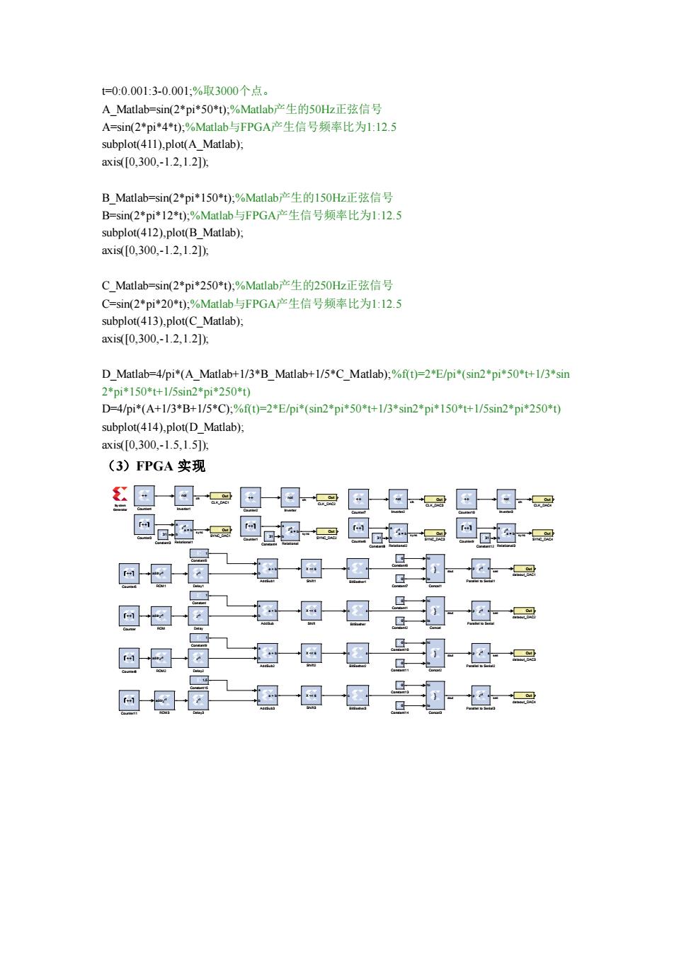
t=0:0.001:3-0.001:%取3000个点。 A_Matlab=-sin(2*pi*50*t);%Matlab产生的50Hz正弦信号 A=sin(2*pi*4*t);%Matlab与FPGA产生信号频率比为1:12.5 subplot(411),plot(A Matlab); axis([0,300,-1.2,1.2] B Matlab=sin(2*pi*150*t);%Matlab产生的150Hz正弦信号 B=sin(2*pi*12*t);%Matlab与FPGA产生信号频率比为1:12.5 subplot(412),plot(B Matlab); axis([0,300,-1.2,1.2]) C_Matlab=sin(2*pi*250*t),%Matlab产生的250Hz正弦信号 C=sin(2*pi*20*t);%Matlab.与FPGA产生信号频率比为1:12.5 subplot(413),plot(C_Matlab); axis([0,300,-1.2,1.2])月 D Matlab=4/pi*(A_Matlab+1/3*B Matlab+1/5*C Matlab);%f(t)=2*E/pi*(sin2*pi*50*t+1/3*sin 2*pi*150*t+1/5sin2*pi*250*t) D=4/pi*(A+1/3*B+1/5*C),%ft)=2*E/pi*(sin2*pi*50*t+1/3*sin2*pi*150*t+1/5sin2*pi*250*t) subplot(414),plot(D Matlab); axis([0,300,-1.5,1.5] (3)FPGA实现 ≤回一回一回是 回一回爱 巴一回受 回④是回是 回最 回g图器 回母量要回昌是0母云 回昌日g昌0 一受 回高-团图-是是0且 晨 晶超日图司回三
t=0:0.001:3-0.001;%取3000个点。 A_Matlab=sin(2*pi*50*t);%Matlab产生的50Hz正弦信号 A=sin(2*pi*4*t);%Matlab与FPGA产生信号频率比为1:12.5 subplot(411),plot(A_Matlab); axis([0,300,-1.2,1.2]); B_Matlab=sin(2*pi*150*t);%Matlab产生的150Hz正弦信号 B=sin(2*pi*12*t);%Matlab与FPGA产生信号频率比为1:12.5 subplot(412),plot(B_Matlab); axis([0,300,-1.2,1.2]); C_Matlab=sin(2*pi*250*t);%Matlab产生的250Hz正弦信号 C=sin(2*pi*20*t);%Matlab与FPGA产生信号频率比为1:12.5 subplot(413),plot(C_Matlab); axis([0,300,-1.2,1.2]); D_Matlab=4/pi*(A_Matlab+1/3*B_Matlab+1/5*C_Matlab);%f(t)=2*E/pi*(sin2*pi*50*t+1/3*sin 2*pi*150*t+1/5sin2*pi*250*t) D=4/pi*(A+1/3*B+1/5*C);%f(t)=2*E/pi*(sin2*pi*50*t+1/3*sin2*pi*150*t+1/5sin2*pi*250*t) subplot(414),plot(D_Matlab); axis([0,300,-1.5,1.5]); (3)FPGA 实现 Out dataout_DAC4 Out dataout_DAC3 Out dataout_DAC2 Out dataout_DAC1 X << 6 Shift3 X << 6 Shift2 X << 6 Shift1 X << 6 Shift Out SYNC_DAC4 Out SYNC_DAC3 Out SYNC_DAC2 Out SYNC_DAC1 a b a = b z - 1 Relational3 a b a = b z - 1 Relational2 a b a = b z - 1 Relational1 a b a = b z - 1 Relational addrz - 1 ROM3 addrz - 1 ROM2 addrz - 1 ROM1 addrz - 1 ROM p z s - 1 Parallel to Serial3 p z s - 1 Parallel to Serial2 p z s - 1 Parallel to Serial1 p z s - 1 Parallel to Serial not Inverter3 not Inverter2 not Inverter1 not Inverter z - 1 Delay3 z - 1 Delay2 z - 1 Delay1 z - 1 Delay ++ Counter9 ++ Counter8 ++ Counter7 ++ Counter6 ++ Counter5 ++ Counter4 ++ Counter3 ++ Counter2 ++ Counter11 ++ Counter10 ++ Counter1 ++ Counter 1 Constant9 3 1 Constant8 0 Constant7 0 Constant6 1 Constant5 3 1 Constant4 3 1 Constant3 0 Constant2 1.5 Constant15 0 Constant14 0 Constant13 3 1 Constant12 0 Constant11 0 Constant10 0 Constant1 1 Constant h i l o } Concat3 h i l o } Concat2 h i l o } Concat1 h i l o } Concat Out CLK_DAC4 Out CLK_DAC3 Out CLK_DAC2 Out CLK_DAC1 c a BitBasher3 c a BitBasher2 c a BitBasher1 c a BitBasher a b a + b AddSub3 a b a + b AddSub2 a b a + b AddSub1 a b a + b AddSub Sy stem Generator sy nc clk dout seri sy nc clk dout seri sy nc clk dout seri sy nc clk dout seri