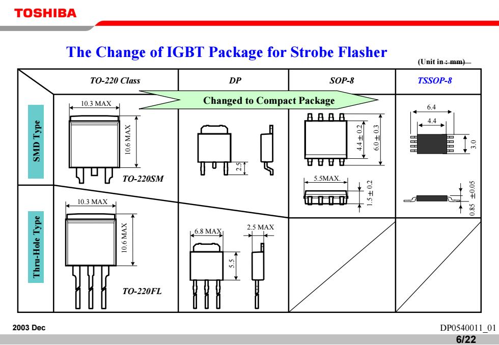
TOSHIBA The Change of IGBT Package for Strobe Flasher (Unit in:mm) TO-220 Class DP SOP-8 TSSOP-8 10.3 MAX Changed to Compact Package 6.4 BBRB ZOFFF ¥44 80103 1 日日日g T0-220SM 5.5MAX. S00 10.3 MAX 兰 L6.8 MAX 2.5 MAX T0-220FL 2003 Dec DP054001101 6122
6/22 2003 Dec DP0540011_01 Thru-Hole Type SMD Type (Unit in : mm) DP The Change of IGBT Package for Strobe Flasher TO-220 Class SOP-8 TSSOP-8 Changed to Compact Package TO-220FL TO-220SM 2.5 10.3 MAX 10.6 MAX 10.3 MAX 10.6 MAX 6.8 MAX 5.5 2.5 MAX 4.4 ±0.2 6.0 ±0.3 5.5MAX. 1.5 ±0.2 3.0 6.4 4.4 0.85 ±0.05
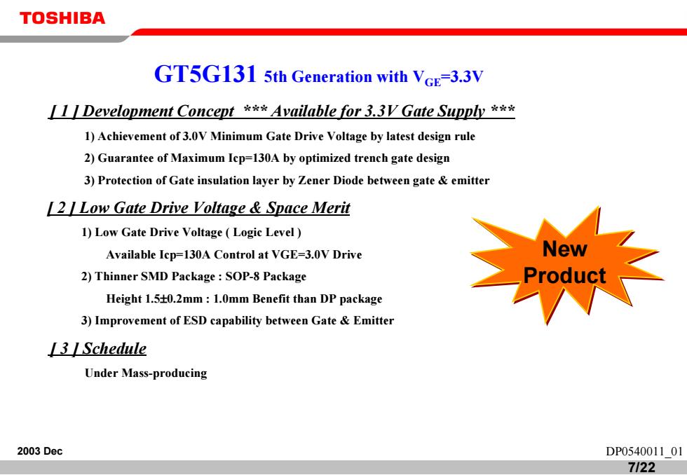
TOSHIBA GT5G131 5th Generation with VGe=3.3V [1 Development Concept **Available for 3.3V Gate Supply ** 1)Achievement of 3.0V Minimum Gate Drive Voltage by latest design rule 2)Guarantee of Maximum Icp=130A by optimized trench gate design 3)Protection of Gate insulation layer by Zener Diode between gate emitter 2 I Low Gate Drive Voltage Space Merit 1)Low Gate Drive Voltage(Logic Level) Available Icp=130A Control at VGE=3.0V Drive 2)Thinner SMD Package SOP-8 Package Height 1.540.2mm 1.0mm Benefit than DP package 3)Improvement of ESD capability between Gate Emitter 米 L3 ISchedule Under Mass-producing 2003 Dec DP054001101 7122
7/22 2003 Dec DP0540011_01 [ 1 ] Development Concept *** Available for 3.3V Gate Supply *** 1) Achievement of 3.0V Minimum Gate Drive Voltage by latest design rule 2) Guarantee of Maximum Icp=130A by optimized trench gate design 3) Protection of Gate insulation layer by Zener Diode between gate & emitter [ 2 ] Low Gate Drive Voltage & Space Merit 1) Low Gate Drive Voltage ( Logic Level ) Available Icp=130A Control at VGE=3.0V Drive 2) Thinner SMD Package : SOP-8 Package Height 1.5±0.2mm : 1.0mm Benefit than DP package 3) Improvement of ESD capability between Gate & Emitter [ 3 ] Schedule Under Mass-producing GT5G131 5th Generation with VGE=3.3V New Product New Product
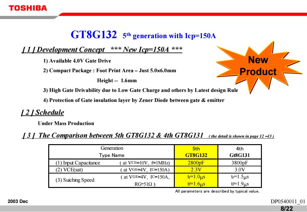
TOSHIBA GT8G132 5th generation with Icp=150A [1 Development Concept **New Icp=150A ** 1)Available 4.0V Gate Drive 2)Compact Package Foot Print Area-Just 5.0x6.0mm Height-1.6mm 3)High Gate Drivability due to Low Gate Charge and others by Latest design Rule 4)Protection of Gate insulation layer by Zener Diode between gate emitter 2 I Schedule Under Mass Production 13I The Comparison between 5th GT8G132 4th GT8G131 (the detail is shown in page 12-13) Generation 5th 4th Type Name GT8G132 Gt8G131 (1)Input Capacitance at VCE=10V,f=IMHz) 2800pF 3800pF (2)VCE(sat) at VGE=4V,IC=150A) 2.3V 3.0V (3)Suiching Speed at VGE=4V,IC=150A, t=1.0μs te1.5μs RG=512) tf=1.6us tf=1.9us All parameters are described by typical value. 2003 Dec DP054001101 8/22
8/22 2003 Dec DP0540011_01 [ 1 ] Development Concept *** New Icp=150A *** 1) Available 4.0V Gate Drive 2) Compact Package : Foot Print Area – Just 5.0×6.0mm Height - 1.6mm 3) High Gate Drivability due to Low Gate Charge and others by Latest design Rule 4) Protection of Gate insulation layer by Zener Diode between gate & emitter [ 2 ] Schedule Under Mass Production [ 3 ] The Comparison between 5th GT8G132 & 4th GT8G131 ( the detail is shown in page 12 ∼13 ) GT8G132 5th generation with Icp=150A New Product New Product 5th 4th GT8G132 Gt8G131 (1) Input Capacitance ( at VCE=10V, f=1MHz) 2800pF 3800pF (2) VCE(sat) ( at VGE=4V, IC=150A) 2.3V 3.0V ( at VGE=4V, IC=150A, tr=1.0µs tr=1.5µs RG=51Ω ) tf=1.6µs tf=1.9µs Generation Type Name All parameters are described by typical value. (3) Suiching Speed