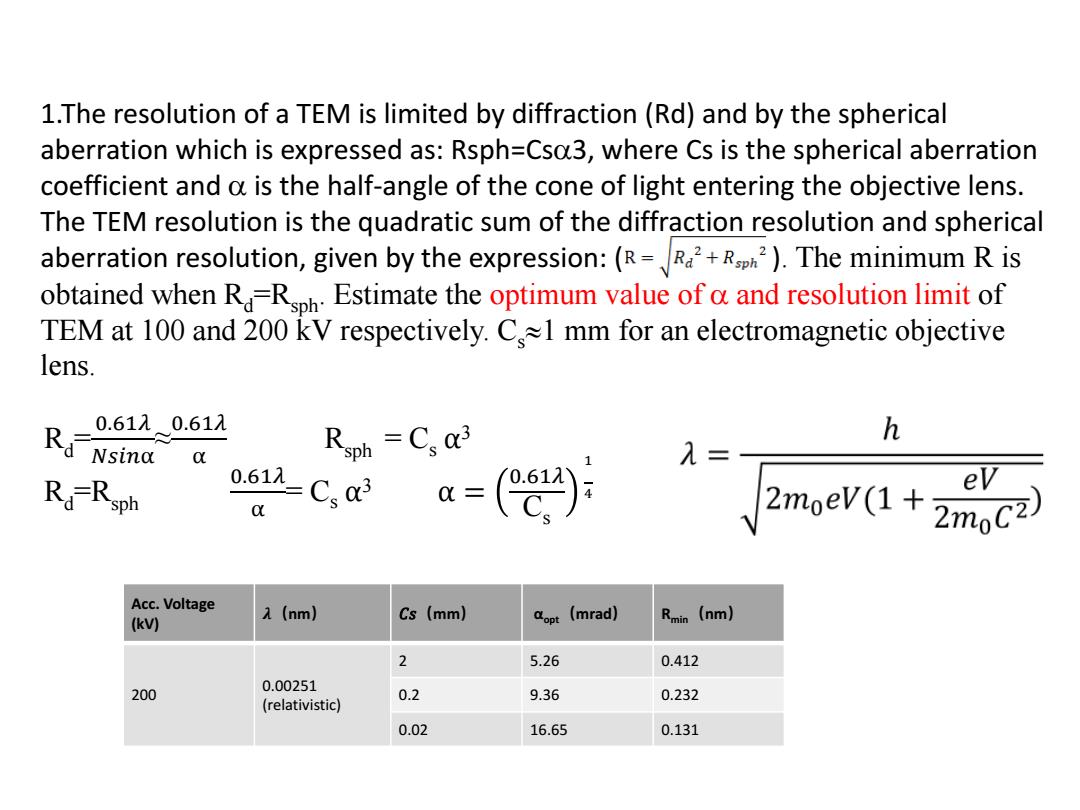
1.The resolution of a TEM is limited by diffraction(Rd)and by the spherical aberration which is expressed as:Rsph=Csa3,where Cs is the spherical aberration coefficient and a is the half-angle of the cone of light entering the objective lens. The TEM resolution is the quadratic sum of the diffraction resolution and spherical aberration resolution,given by the expression:(R=Ra2+Rp2).The minimum R is obtained when RRhEstimate the optimum value of a and resolution limit of TEM at 100 and 200 kV respectively.C 1 mm for an electromagnetic objective lens. 0.6110.617 Rd Nsinc h Ri-Rsph 061-C,a= C (+ Acc.Voltage (kv) (nm) Cs (mm) dopt (mrad) Rmin (nm) 2 5.26 0.412 200 0.00251 0.2 9.36 0.232 (relativistic) 0.02 16.65 0.131
1.The resolution of a TEM is limited by diffraction (Rd) and by the spherical aberration which is expressed as: Rsph=Cs3, where Cs is the spherical aberration coefficient and is the half-angle of the cone of light entering the objective lens. The TEM resolution is the quadratic sum of the diffraction resolution and spherical aberration resolution, given by the expression: ( ). The minimum R is obtained when Rd =Rsph. Estimate the optimum value of and resolution limit of TEM at 100 and 200 kV respectively. Cs 1 mm for an electromagnetic objective lens. Rd = 0.61𝜆 𝑁𝑠𝑖𝑛α ≈ 0.61𝜆 α Rsph = Cs α 3 Rd =Rsph 0.61𝜆 α = Cs α 3 α = 0.61𝜆 Cs 1 4 Acc. Voltage (kV) 𝝀(nm) 𝐶𝑠(mm) αopt(mrad) Rmin(nm) 200 0.00251 (relativistic) 2 5.26 0.412 0.2 9.36 0.232 0.02 16.65 0.131
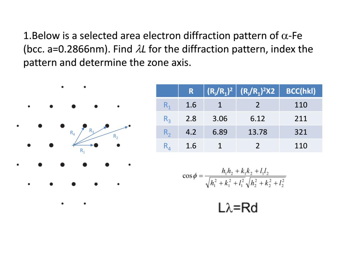
1.Below is a selected area electron diffraction pattern of a-Fe (bcc.a=0.2866nm).Find AL for the diffraction pattern,index the pattern and determine the zone axis. R (R/R2 (R:/R)2X2 BCC(hkl) Ri 1.6 1 2 110 R3 2.8 3.06 6.12 211 R 4.2 6.89 13.78 321 R> R2 Ra 1.6 1 2 110 cos中= hh2+k k2 +1l2 Vh+k+Vn好+k好+ Lλ=Rd
1.Below is a selected area electron diffraction pattern of -Fe (bcc. a=0.2866nm). Find L for the diffraction pattern, index the pattern and determine the zone axis. R (Ri /R1 ) 2 (Ri /R1 ) 2X2 BCC(hkl) R1 1.6 1 2 110 R3 2.8 3.06 6.12 211 R2 4.2 6.89 13.78 321 R4 1.6 1 2 110 R1 R2 R R3 4
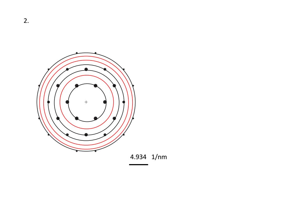
2. 4.9341/nm
2. 4.934 1/nm
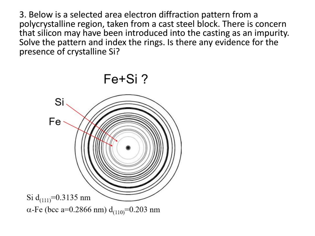
3.Below is a selected area electron diffraction pattern from a polycrystalline region,taken from a cast steel block.There is concern that silicon may have been introduced into the casting as an impurity. Solve the pattern and index the rings.Is there any evidence for the presence of crystalline Si? Fe+Si Si Fe Si da=0.3135 nm a-Fe (bcc a=0.2866 nm)d(o)=0.203 nm
3. Below is a selected area electron diffraction pattern from a polycrystalline region, taken from a cast steel block. There is concern that silicon may have been introduced into the casting as an impurity. Solve the pattern and index the rings. Is there any evidence for the presence of crystalline Si?
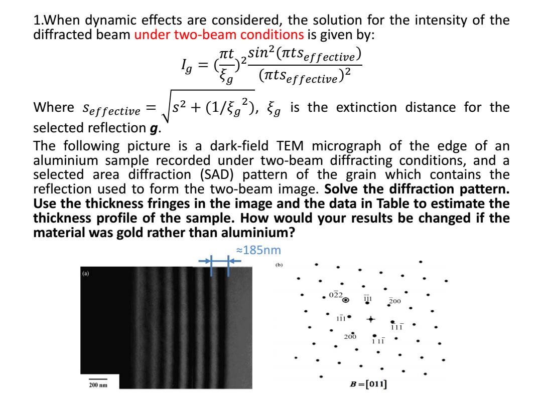
1.When dynamic effects are considered,the solution for the intensity of the diffracted beam under two-beam conditions is given by: 1g= ((seei) (πtSeffective)Z Where Seffective=s2+(1/5g2),g is the extinction distance for the selected reflection g. The following picture is a dark-field TEM micrograph of the edge of an aluminium sample recorded under two-beam diffracting conditions,and a selected area diffraction (SAD)pattern of the grain which contains the reflection used to form the two-beam image.Solve the diffraction pattern. Use the thickness fringes in the image and the data in Table to estimate the thickness profile of the sample.How would your results be changed if the material was gold rather than aluminium? ≈185nm (b) (a) 02 200nm B=[011]
1.When dynamic effects are considered, the solution for the intensity of the diffracted beam under two-beam conditions is given by: 𝐼𝑔 = ( 𝜋𝑡 𝜉𝑔 ) 2 𝑠𝑖𝑛2 (𝜋𝑡𝑠𝑒𝑓𝑓𝑒𝑐𝑡𝑖𝑣𝑒) (𝜋𝑡𝑠𝑒𝑓𝑓𝑒𝑐𝑡𝑖𝑣𝑒) 2 Where 𝑠𝑒𝑓𝑓𝑒𝑐𝑡𝑖𝑣𝑒 = 𝑠 2 + (1/𝜉𝑔 2 ), 𝜉𝑔 is the extinction distance for the selected reflection g. The following picture is a dark-field TEM micrograph of the edge of an aluminium sample recorded under two-beam diffracting conditions, and a selected area diffraction (SAD) pattern of the grain which contains the reflection used to form the two-beam image. Solve the diffraction pattern. Use the thickness fringes in the image and the data in Table to estimate the thickness profile of the sample. How would your results be changed if the material was gold rather than aluminium? ≈185nm