《IC封装设计与仿真》 ” QQ:402977009 群:24640973
www.chinafastprint.com 《IC封装设计与仿真》 QQ:402977009 群:24640973

1.IC封装设计 2.封装电磁仿真 3.封装热仿真 4.封装结构仿真
www.chinafastprint.com 1.IC封装设计 3.封装热仿真 2.封装电磁仿真 内容 4.封装结构仿真

1.IC封装设计
www.chinafastprint.com 1.IC封装设计

IC封装设计 IC封装内部结构: DIP (Dual In-line Package) SIP 正面 Pin脚 塑封 背面 SSOP Mold resin OKI JAPAN Chip 晶体 7578H (Shrink Small 5012902 Outline Package)Gold wire 芯片 5的的的的的的 Lead 金线 RLC元件 基板 QFP Chip // (Quad Flat Package) Gold wire 4 Mold resin Lead
www.chinafastprint.com IC封装内部结构: IC封装设计 塑封 金线 基板 芯片 RLC元件 晶体 Pin脚
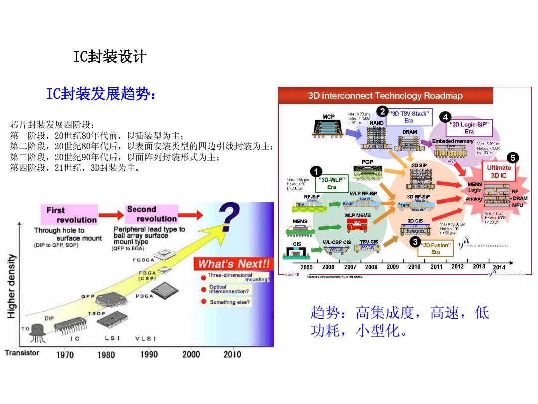
IC封装设计 IC封装发展趋势: 3D interconnect Technology Roadmap MCP Vis:>20 um 2“3 D TSV Stack' 4 芯片封装发展四阶段: t=5约mAND Era 3D Logic-SiP" 第一阶段,20世纪80年代前,以插装型为主: DRAM Era 第二阶段,20世纪80年代后,以表面安装类型的四边引线封装为主: Embeded memory 52』 第三阶段,20世纪90年代后,以面阵列封装形式为主: 0000007 POP 5 第四阶段,21世纪,3D封装为主。 3D SIP Ultimate 3D IC "3D-WLP" Era MEMS Logic RF-SiP WLP RF.SiP 3D RF.SiP Analog DRAM Psse Passive First Second E WLP MEMS Mas<1um revolution revolution Haks 100K ME日MS 3D CIs Vies=10-30 um 1e20m Through hole to Peripheral lead type to Hoesc10 nenn t<50m surface mount ball array surface (DIP to QFP,SOP) mount type CIS WL-CSP CIS TSVCIS 3 3D Fusion' (QFP to BGA) 9000s7 Era FCBGA What's Next!! F台GA 20052006 2007 2008 2009 2010 2011 20122013 2014 Three-dimensional (CSP) mounting? Optical interconnection? OF P PBGA ●Something else7 趋势:高集成度,高速,低 DIP 功耗,小型化。 LSI VLSI Transistor 1970 1980 1990 2000 2010
www.chinafastprint.com IC封装发展趋势: IC封装设计 趋势:高集成度,高速,低 功耗,小型化。 芯片封装发展四阶段: 第一阶段,20世纪80年代前,以插装型为主; 第二阶段,20世纪80年代后,以表面安装类型的四边引线封装为主; 第三阶段,20世纪90年代后,以面阵列封装形式为主; 第四阶段,21世纪,3D封装为主